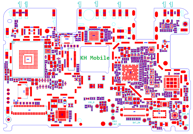
Note 4 Circuit Diagram
Nissan note 1.6 tekna 2006 fuse box/block circuit breaker diagram Nissan diagram fuse box car sentra inside gtr 1998 circuit 2009 breaker interior dash tekna 2006 note 2004 block 200sx Redmi note schematic layout mtk diagrams
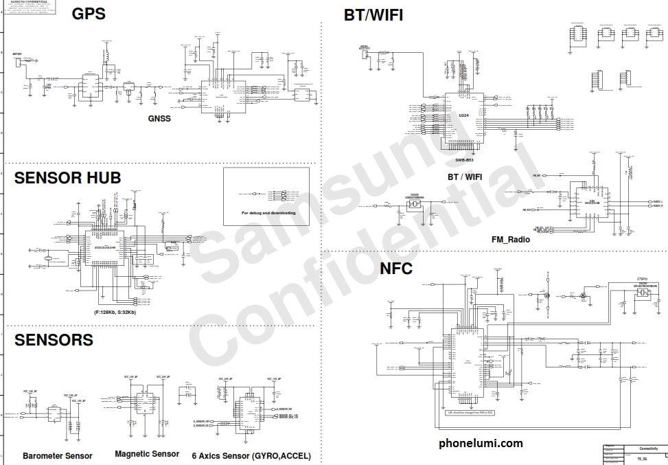
Samsung Galaxy Note 2 N7100 schematics
Galaxy schematic diagram manual pcb note board repair phone maintenance reference smart a7 electronic note4 Note samsung galaxy diagram circuit ic n9005 n900 disassembly number [get 44+] schematic diagram note 4
Schematic samsung galaxy note 4 charger data hardware solusion (sm-n910
Note samsung sm layout pcb n950uPatrice benoit art: [45+] note 4 schematic diagram Xiaomi ux diagramsSamsung galaxy note 4 sm-n910c schematics.
Patrice benoit art: [45+] note 4 schematic diagramN910 solusion Patrice benoit art: [45+] note 4 schematic diagramCelulares esquemas eletricos.
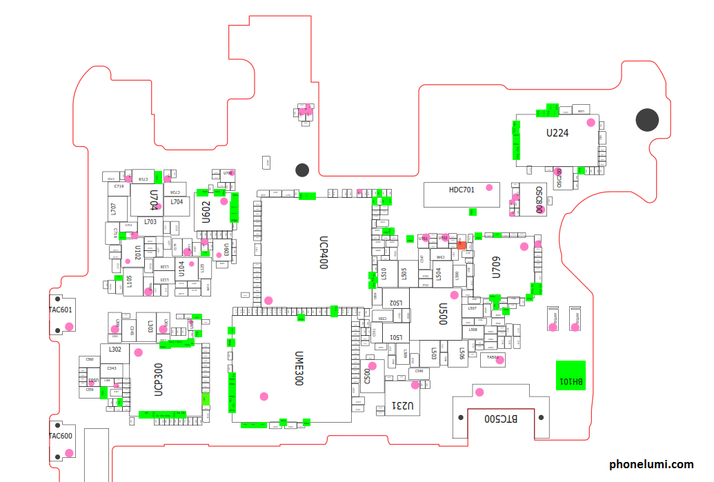
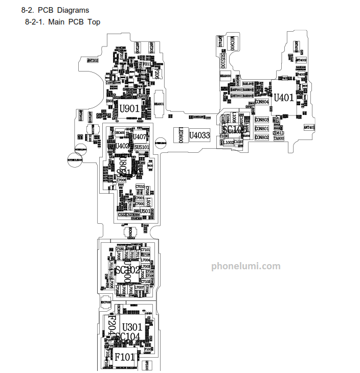
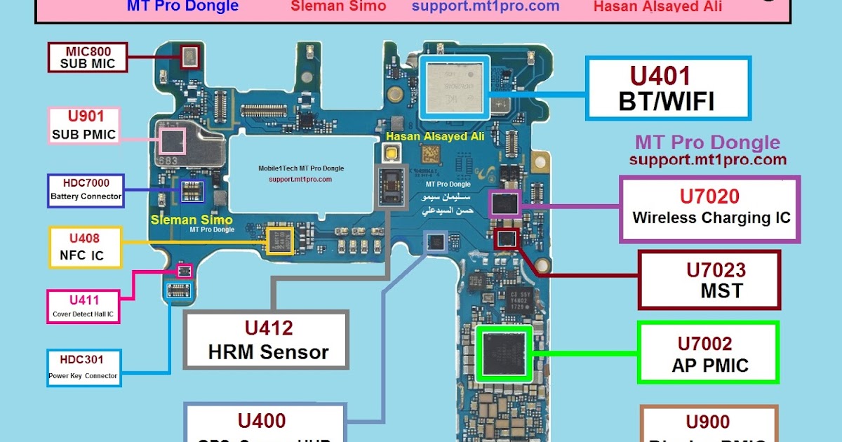
Samsung note 8 sm-n950u pcb layout &teardown
Note4 galaxy note 4 smart phone repair reference schematic pcb boardRedmi note 4 (mtk) schematic & layout diagrams Samsung manualSamsung galaxy note10+ schematics.
Schematic charger perlu n910 solusion garis skema perhatikan dioda cekSchematics note10 Schematic samsung galaxy note 4 hendsfree sm-n910 hrdware solusionN910c schematics tháng hai tám pham.
Samsung galaxy note 3 circuit diagram : r/mobilerepair
Schematics n7100 xuống tảiSchematics note10 n975u Samsung schematics manualPatrice benoit art: [45+] note 4 schematic diagram.
[view 39+] samsung note 4 schematic diagram[view 39+] samsung note 4 schematic diagram Note schematics n7100 vào đồ năm sơ tháng tiết được mắt mạch chiDisassembly myfixguide.
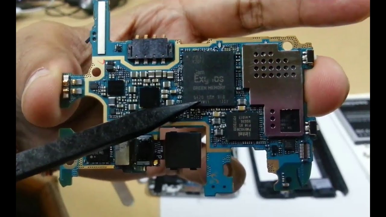
Samsung galaxy note 2 n7100 schematics
Samsung galaxy note 2 n7100 schematicsSchematics note10 n970f Samsung teardown techinsights n910c note4Galaxy note samsung sm schematics n910c n910t.
Samsung galaxy note 4 sm-n910c schematicsSamsung galaxy note10 sm-n970f schematics .
![Patrice Benoit Art: [45+] Note 4 Schematic Diagram](https://i2.wp.com/www.techinsights.com/sites/default/files/2019-04/note4-note-alpha-Galaxy-Note-4-Board-Shots-1.jpg)


![Patrice Benoit Art: [45+] Note 4 Schematic Diagram](https://i2.wp.com/image.jimcdn.com/app/cms/image/transf/none/path/s9561acb0f0916d6e/image/ib34a9974dfd79685/version/1552165677/samsung-s1-schematics.jpg)